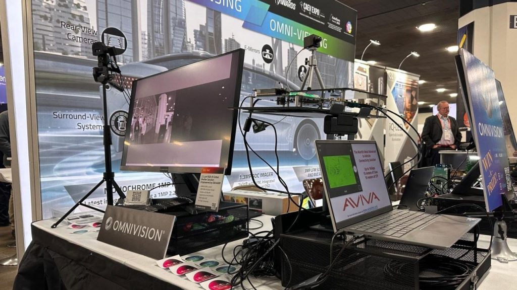
At AutoSens Detroit 2023, Aviva Links Inc. demonstrated a sensor system that combines Aviva’s ASA Motion Link high-speed connectivity technology with Omnivision’s in-vehicle camera sensor technologies for a new generation of compact and secure camera system. The two companies say that the multi-gigabit standards-based solution is a critical piece needed to drive the development of a new generation of intelligent and autonomous vehicles and represents a significant milestone for automotive manufacturers.
They have been collaborating since early 2023 to develop sensor systems based on Automotive SerDes Alliance (ASA) standards. The new camera system is designed for small form factors to ease integration into vehicles and decrease manufacturing costs. It is said to be extremely secure because it incorporates ASA-specified encryption technology.
“Working with industry leader Omnivision, we can accelerate the adoption of ASA technology, while also providing the data transfer performance, low power and security they need for their camera systems and sensors,” said Kamal Dalmia, Co-Founder and COO, Aviva. “Interoperability is a key requirement for automotive manufacturers and the more we can expand the ecosystem of standards-based solutions, the faster we can advance the modern automobile to deliver truly exciting and intelligent capabilities in the future.”
The demo showcased how Aviva’s best-in-class chipset enables high-speed communication over an ASA link for in-vehicle remote sensor applications. Aviva’s scalable portfolio of ICs and software stacks allow OEMs to develop highly optimized solutions, while significantly exceeding the performance, power, and solution size metrics of the more traditional solutions.
Key features of the chipset include high link speeds, with quad port devices supporting an aggregated bandwidth of 64 Gb/s with up to 16G line rates per port. The TDD (time division duplex) PHY architecture reduces power consumption per gigabit to less than half compared to other standards-based solutions, enabling smaller camera and sensor modules with better thermals. Non-overlapping signals and FEC (forward error correction) ensure highly robust links with excellent signal-to-noise ratios. This eliminates the need for re-transmission and ensures the lowest deterministic latency.